Diodes: Difference between revisions
(added diode diag more to come) |
|||
| (8 intermediate revisions by one other user not shown) | |||
| Line 1: | Line 1: | ||
Related wiki pages: [[Electronic Theory]], [[Current]], [[Voltage]], [[Bipolar-Junction Transistors]], [[Field Effect Transistors (FETs)]] | |||
==What is a diode?== | |||
In its simplest state, a diode is an electrical device that allows current to flow in one direction but not the other. | |||
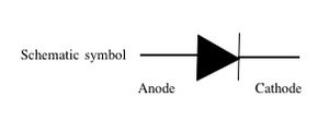
===What is the circuit symbol for a diode?=== | |||
[[Image:vk4yeh_diode_symbol.jpg | 300px]] | |||
==What is a diode made of?== | |||
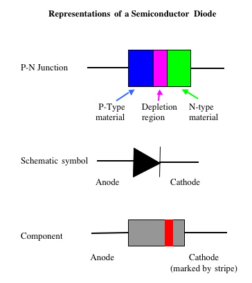
Semiconductor diodes are constructed of layer of [http://en.wikipedia.org/wiki/N-type_semiconductor N-Type] semiconducting material joined to a layer of [http://en.wikipedia.org/wiki/P-type_semiconductor P-Type] semicondictor material. Beteen these is a [http://en.wikipedia.org/wiki/Depletion_region depletion layer] that varies in thickness depending of the voltage bias across the diode. | |||
===How does the structure of a diode relate to its circuit symbol?=== | |||
[[Image:vk4yeh diode 1.jpg |400px]] | [[Image:vk4yeh diode 1.jpg |400px]] | ||
==What are the electrical characteristics of a diode?== | |||
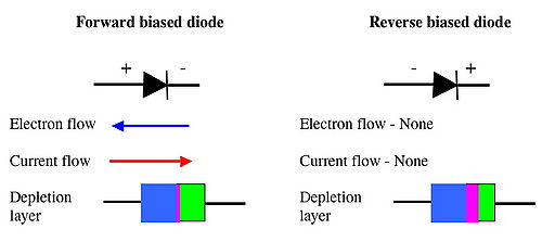
A diode is analogous to a valve or switch that only allows electrons to flow in one direction. When the anode is more positive than the cathode, the diode is said to be'''forward bised''', and electrons can flow from cathode to anode. (conventional current is said to flow in the opposite direction). In this orientation the depletion layer becomes very thin (the valve opens) | |||
When the cathode is more positive than the anode, the depletion layer becomes much wider, preventing the flow of electrons and hence stopping current flow. | |||
[[Image:Vk4yeh_diode-2.jpg | 500px]] | |||
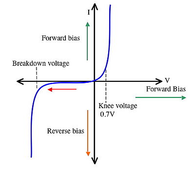
A voltage of approximately 0.7V is required to narrow the depletion layer sufficiently for current to flow. If a diode is reverse biased with sufficient voltage it will break down completely. This is known as the '''P'''eak '''I'''nverse '''V'''oltage or PIV | |||
[[Image:Vk4yeh_diode_graph.jpg |400px]] | |||
==What do the diode ratings mean?== | |||
*'''Maximum repetitive reverse voltage''' - <Math>V_{RRM}</math>, the maximum repeatedly pulsed voltage the diode can withstand in reverse-bias mode. | |||
* '''Maximum DC reverse voltage''' - <Math>V_R</math> or <Math>V_{DC}</math>, the maximum continuous DC voltage the diode can withstand in reverse-bias mode. | |||
* '''Maximum forward voltage''' - <Math>V_F</math>, usually specified at the diode's rated forward current. | |||
* '''Maximum (average) forward current''' - <Math>I_{F(AV)}</math>, the maximum average current the diode is able to conduct in forward bias mode. This is limited by the thermal limitation: characteristics of the diode. | |||
* '''Maximum (peak or surge) forward current''' - <Math>I_{FSM}</math> or <Math>i_{f(surge)}</math>, the maximum peak current the diode is able to conduct in forward bias mode. | |||
* '''Maximum total dissipation''' - <Math>P_D</math>, the maximum power (in watts)that the diode can dissipate. This is limited by the thermal characteristics of the diode. | |||
* '''Operating junction temperature''' - <Math>T_J</math>, the maximum allowable temperature for the diode's PN junction, usually given in degrees Celsius | |||
* '''Storage temperature range''' - <Math>T_{STG}</math>, the range of allowable temperatures for storing an unpowered diode. Usually the maximum storage temperature will be the same as the maximum junction temerature. | |||
* '''Thermal resistance''' - R(Θ), the temperature difference between the junction and the surrounding air or between junction and leads, for a given power dissipation. Expressed in units of degrees Celsius per watt. | |||
* '''Maximum reverse current''' - <Math>I_R</math> , the current through the diode in reverse-bias mode, when the maximum rated inverse voltage <Math>V_{DC} </math> is applied (VDC). This is also known as the '''leakage current'''. | |||
* '''Typical junction capacitance''' - <Math>C_J</math>, the capacitance of the junction due to the depletion region acting as a dielectric separating the P and N layers. | |||
* '''Reverse recovery time''' - <Math>t_rr</math>, the time it takes for a diode to “turn off” when the voltage across it alternates from forward-bias to reverse-bias polarity. | |||
==Diode types== | |||
[[Image:Vk4yeh_diodes.jpg |400px]] | |||
` | |||
{{electronics}} | |||
Latest revision as of 18:20, 8 April 2009
Related wiki pages: Electronic Theory, Current, Voltage, Bipolar-Junction Transistors, Field Effect Transistors (FETs)
What is a diode?
In its simplest state, a diode is an electrical device that allows current to flow in one direction but not the other.
What is the circuit symbol for a diode?
What is a diode made of?
Semiconductor diodes are constructed of layer of N-Type semiconducting material joined to a layer of P-Type semicondictor material. Beteen these is a depletion layer that varies in thickness depending of the voltage bias across the diode.
How does the structure of a diode relate to its circuit symbol?
What are the electrical characteristics of a diode?
A diode is analogous to a valve or switch that only allows electrons to flow in one direction. When the anode is more positive than the cathode, the diode is said to beforward bised, and electrons can flow from cathode to anode. (conventional current is said to flow in the opposite direction). In this orientation the depletion layer becomes very thin (the valve opens)
When the cathode is more positive than the anode, the depletion layer becomes much wider, preventing the flow of electrons and hence stopping current flow.
A voltage of approximately 0.7V is required to narrow the depletion layer sufficiently for current to flow. If a diode is reverse biased with sufficient voltage it will break down completely. This is known as the Peak Inverse Voltage or PIV
What do the diode ratings mean?
- Maximum repetitive reverse voltage - <Math>V_{RRM}</math>, the maximum repeatedly pulsed voltage the diode can withstand in reverse-bias mode.
- Maximum DC reverse voltage - <Math>V_R</math> or <Math>V_{DC}</math>, the maximum continuous DC voltage the diode can withstand in reverse-bias mode.
- Maximum forward voltage - <Math>V_F</math>, usually specified at the diode's rated forward current.
- Maximum (average) forward current - <Math>I_{F(AV)}</math>, the maximum average current the diode is able to conduct in forward bias mode. This is limited by the thermal limitation: characteristics of the diode.
- Maximum (peak or surge) forward current - <Math>I_{FSM}</math> or <Math>i_{f(surge)}</math>, the maximum peak current the diode is able to conduct in forward bias mode.
- Maximum total dissipation - <Math>P_D</math>, the maximum power (in watts)that the diode can dissipate. This is limited by the thermal characteristics of the diode.
- Operating junction temperature - <Math>T_J</math>, the maximum allowable temperature for the diode's PN junction, usually given in degrees Celsius
- Storage temperature range - <Math>T_{STG}</math>, the range of allowable temperatures for storing an unpowered diode. Usually the maximum storage temperature will be the same as the maximum junction temerature.
- Thermal resistance - R(Θ), the temperature difference between the junction and the surrounding air or between junction and leads, for a given power dissipation. Expressed in units of degrees Celsius per watt.
- Maximum reverse current - <Math>I_R</math> , the current through the diode in reverse-bias mode, when the maximum rated inverse voltage <Math>V_{DC} </math> is applied (VDC). This is also known as the leakage current.
- Typical junction capacitance - <Math>C_J</math>, the capacitance of the junction due to the depletion region acting as a dielectric separating the P and N layers.
- Reverse recovery time - <Math>t_rr</math>, the time it takes for a diode to “turn off” when the voltage across it alternates from forward-bias to reverse-bias polarity.
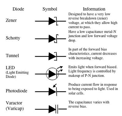
Diode types
| Electronic Theory | |
| Physical quantities | Current * Gain * Impedance * Power * Q of a circuit * Radiated Power Measurement * Reactance* Resistivity * Resonance * Voltage |
| Components | Baluns * Bipolar-Junction Transistors * Capacitors * Diodes * Inductors* Lasers * Microphones * Resistors * Transformers * Wire |
| Circuits | Attenuators * Digital Signal Processing (DSP) * Dummy load * Filters * LC filters * Power Supply Design * Rectifier Circuits |
| Design | Amplifier Design * Oscillator Design |
| Electromagnetic Waves | Relative power (Decibels) * Harmonics * Interference and BPL |
